
Single-Crystal Wafers & Substrates
Silicon IR Optical Substrates & Wafers
Single-crystal silicon substrates for CO₂ laser mirrors and selected IR optics, alongside research wafers with specified orientation, surface finish, and resistivity.
- Germany-based supplier and manufacturing partner
- Manufacturing to customer specifications
- Optical inspection and measurement against specified requirements
- From single components and prototypes to repeat supply
Product overview
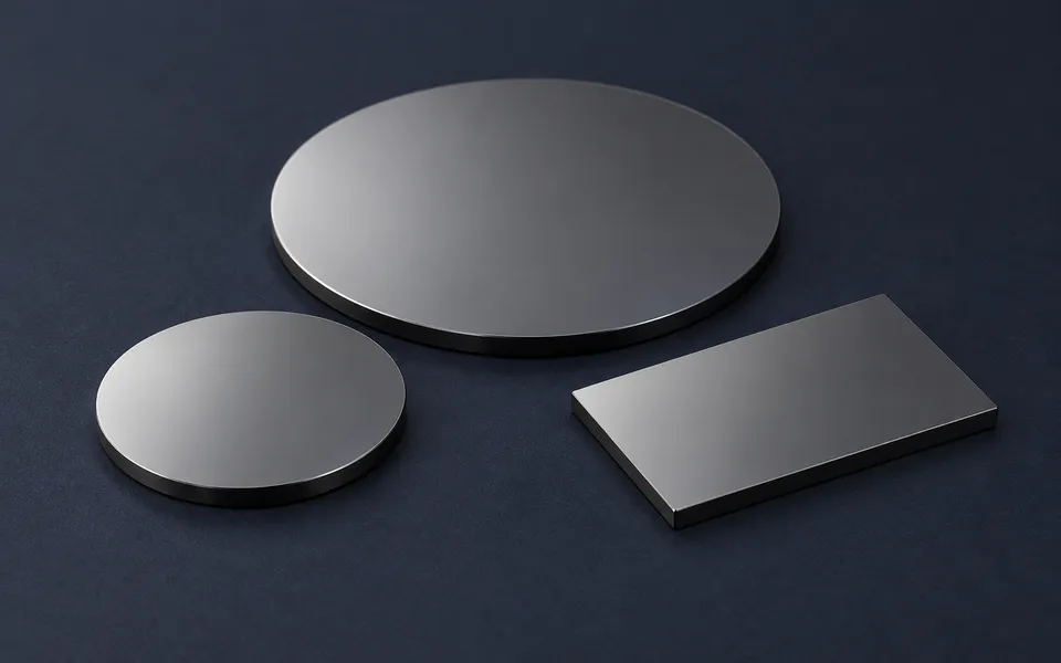
Our product scope includes custom silicon mirror substrates and single-crystal silicon wafers. Depending on the application, specifications may include crystal orientation, dimensions, thickness, surface finish, and, where relevant, conductivity type, dopant, and electrical resistivity.
Single-crystal silicon (Si) is used for infrared optical substrates, mirror blanks, and research wafers. Its high thermal conductivity, low thermal expansion, and relatively low density make it suitable for selected reflective optical applications, including substrates for CO₂ laser mirrors operating at 10.6 µm.
Silicon is also used for transmissive infrared windows at suitable wavelengths. However, transmission performance depends on material grade, crystal growth method, electrical resistivity, thickness, and operating wavelength.
Wafer specifications and infrared optical transmission requirements should be specified and evaluated separately.
Key advantages
- High thermal conductivity for effective heat dissipation
- Low thermal expansion for dimensional stability under temperature changes
- Relatively low density for weight-sensitive infrared optical systems
- High hardness for wear resistance in suitable applications
Typical specifications
| Crystal growth method | Czochralski (CZ) |
|---|---|
| Diameter | 200 mm; other sizes on request |
| Diameter tolerance | ±0.2 mm |
| Thickness | On request |
| Conductivity type / dopant | p-type (boron-doped) / n-type (phosphorus-doped) |
| Crystal orientation | (100) / (111) |
| Electrical resistivity | 0.1–50 Ω·cm |
| Total Indicator Reading (TIR) | < 2.0 µm |
| Maximum Site Total Indicator Reading (STIRmax) | < 0.3 µm |
| Warp | < 20 µm |
Typical applications
- Infrared and CO₂ laser mirror substrates
- Uncoated mirror blanks for custom reflective optics
- Reflective optical components for thermally demanding laser systems
- Selected infrared windows for imaging, sensing, and optical instrumentation
- Silicon wafers for research and thin-film applications, subject to wafer grade and process requirements
View related products

Optical Mirrors
Flat, wedged, curved, and aspherical geometries with HR, PR, output-coupler, dichroic, and multi-wavelength coatings.

Optical Windows
Flat, wedged, tubular, and Brewster window configurations, including chip-free, unchamfered edge options.

Optical Lenses
Spherical, cylindrical, aspherical, wedged, and rectangular lens geometries with specified surface quality, centration, and coatings.
Sapphire Wafers & Substrates
For thin-film deposition and epitaxial research, with options for custom crystal orientations, dimensions, and polished surfaces.
RFQ PREPARATION
What to send for a quote
Please send your drawing or technical specification together with the following information.
- Crystal orientation or cut angle and required dimensions
- Thickness, dimensional tolerances, and geometry requirements
- Required miscut (off-axis) angle and direction
- Required surface roughness and surface-finish specification
- Required quantity